Focused-Ion Beam Scanning Electron Microscope- looking beneath the surface
News category: Nanotech
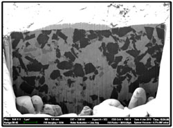
 SEM image of a thin cross section milled out of a sample using the FIB beam of ions. Image courtesy of Dr. James Wesley-Smith
From research on pollen grains to metal oxides, the Focused ion beam scanning electron microscope (FIB SEM) is one of the jewels in the CSIR National Centre for Nano-structured Materials (NCNSM) collection of nanotechnology equipment. Acquired in 2010 the FIB SEM takes the imaging of nanostructures to a new level.
Not only does it allow for the imaging of nano-surfaces similar to the traditional SEM, but it further allows for analysis of internal structures, providing a new precise and almost pure compositional image. It is this feature that sees it benefit all areas of science from material through to the biological sciences.
How does it work? The Auriga Cobra FIB Field Emission SEM instrument at CSIR is a multifunctional instrument that combines SEM imaging with Focused Ion Beam (FIB) milling. In SEM mode, as the beam hits the sample surface it generates secondary electrons. A high resolution secondary electron signal, characteristic of Field Emission instruments, is produced as the beam moves along the surface, and is collected and used to generate an image. The instrument is equipped with a charge compensation system which is used to analyse nonconductive samples without coating, as well as the STEM detector and Energy and Angle Selective EsB detector that allows an almost pure compositional image to be obtained by filtering out unwanted surface information. The FIB column uses a beam of gallium ions for milling a cross section of a sample (see below) or for sputtering, depending on the strength of the beam. The milled cross section can be imaged immediately without breaking the vacuum.
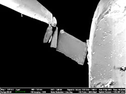
A valuable feature of the FIB SEM is the ability to cut thin layers of the sample (100 nm thickness) for further analysis with a transmission electron microscope (TEM). The FIB SEM is equipped with a Kliendiek micromanipulator which allows the delicate thin lamella cut to be fused to a grid ready to be transferred to a TEM.
Areas of research currently being covered by the FIB-SEM include atomic layer structure visualization of zinc and tin oxides for their use in sensing devices, or to obtain cross sections through hard materials ranging from pollen grains to cutting tools.
Writer: Edith Mshoperi

SEM image of the Kliendiek micromanipulator as it places the lamella onto the TEM for analysis using TEM. Image courtesy of Dr. James Wesley-Smith
